


TF1010 is an electronic-grade ultra-high-purity single-walled carbon nanotube powder prepared by Shandong Tanfeng using super-growth CVD coupled with multi-stage high-temperature deep purification and targeted catalytic impurity removal processes. It is the highest-purity model in the entire single-walled product line, forming a clear gradient distinction from the TF1000 basic single-walled type. The tube diameter is precisely controlled within a narrow distribution range of 1.5–1.7 nm, the pristine carbon tube length is >100 μm, the Raman G/D ratio is >50, and the tube wall amorphous carbon defects are extremely low. The core differentiated indicator: the effective purity of single-walled carbon tubes is >=98.5%, significantly higher than TF1000's 80% purity. Metal ash is gradient-controlled to within the hundred-ppm level, catalyst residual impurities are greatly reduced, fundamentally avoiding semiconductor device leakage, battery side reactions, and sensing signal drift problems.
The seamless tubular structure of single-layer graphene combines ballistic electron conduction, ultra-high elasticity, and ultra-large specific surface area (500–1000 m²/g). The percolation addition amount can be as low as 0.03% to form a full-domain conductive network, suitable for 7 nm and below advanced process thin-film transistors, flexible logic circuits, high-purity silicon-carbon anodes, military and aerospace lightweight shielding, ultra-high-sensitivity trace biosensing, and other high-precision stringent scenarios.
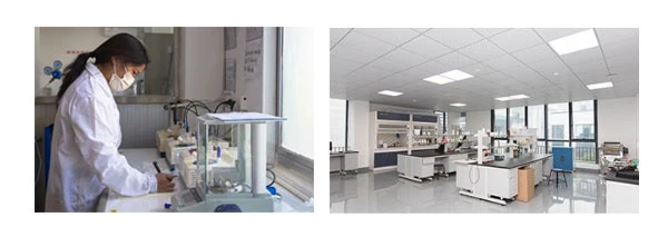
The factory is equipped with a full set of high-purity material dedicated testing equipment including high-resolution TEM, Raman spectroscopy, TGA thermogravimetry, and ICP-OES. Each batch is issued with a full set of special testing reports on single-wall content, metal impurities, tube diameter, and length. Only gram-level high-purity samples and kilogram-level pilot batches are provided to research institutes, semiconductor enterprises, and leading solid-state battery manufacturers. High-purity modified powders with amino and carboxyl groups can be customized to adapt to water/organic solvent dispersion. A full set of RoHS, REACH, high-purity ICP impurity special reports, and MSDS safety data sheets are complete, meeting the stringent material admission audit standards for military and semiconductor import and export.
 |
 |
 |
 |
| 1.5-1.7 nm | ||
| >100 μm | - | |
| Single-Walled Carbon Nanotube Purity | >=98.5% | |
| <=2000 / <500 / <100 ppm | ||
| 500-1000 m²/g | ||
| >50 |

In 2022, the company invested 50 million RMB to establish "Shandong Tanfeng New Materials Technology Co., Ltd." in Heze, Shandong Province, with a building area of 4,000 square meters. It is now a national high-tech enterprise with over ten independent patents.
A second-phase production and R&D center is planned for construction in 2027. The company has passed ISO9001 international quality system certification and has formed an advanced nanomaterial manufacturing and technical service center covering the entire process of operation, R&D, pilot production, and manufacturing. Currently, it possesses complete production lines for carbon nanotube powder, carbon nanotube slurry, carbon nanotube masterbatch, carbon nanotube fiber, and carbon nanotube film.
We have professional testing and certification. For truly nanoscale carbon nanotubes, Tanfeng Technology provides characterization data for various models, such as SEM images, AFM images, HRTEM images, Raman spectroscopy, and X-ray powder diffraction patterns.
 |
 |
 |
 |
Single-wall purity >=98.5%, extremely low impurity and miscellaneous tube content, adapting to semiconductor device on/off ratio requirements
Compared to TF1000's single-wall purity of only 80%, TF1010 removes multi-walled carbon tubes and amorphous carbon particles through multi-stage purification, with miscellaneous phase impurities accounting for less than 1.5%. When used in thin-film field-effect transistors, the device on/off ratio is increased by more than 10 times, with no leakage or signal distortion caused by metallic miscellaneous tubes, adapting to the research and development of 7 nm and below advanced carbon-based integrated circuits.
Three grades of ultra-low metal ash available, completely solving the failure problem of trace metal ion migration
<100 ppm / <500 ppm / <2000 ppm. Military and semiconductor chips can choose the ultra-pure grade within 100 ppm. Eliminates catalyst metal residue precipitating during device energization, avoiding wafer short circuits, continuous solid-state battery side reactions, and sensor baseline drift.
1.5–1.7 nm narrow tube diameter distribution + >100 μm ultra-long pristine tubes, extremely low filling without blocking light transmission
Ten-thousand-level ultra-high aspect ratio, conductive addition amount as low as 0.03%, filler dosage reduced by another 30% compared to TF1000 for the same conductive effect. Tube diameter is far smaller than visible light wavelength, preparing transparent conductive films with no haze and high transmittance, adapting to mass production of foldable screens and photovoltaic transparent electrodes.
Ultra-high crystallinity G/D >50, extremely few tube wall structural defects, electrochemical cycle stability maximized
Low-defect graphene tube walls reduce electrolyte interface side reactions. When used in silicon-carbon anodes and solid-state batteries, they can greatly suppress continuous SEI film thickening, with cell cycle life improved by more than 35% compared to TF1000 basic single-walled, adapting to long-range high-end passenger vehicle power batteries.
Can directionally separate semiconducting single-walled carbon tubes, core substrate for low-power flexible chips
High-purity pristine single-walled raw materials facilitate subsequent density gradient centrifugation separation, producing a high proportion of semiconducting single-walled carbon nanotubes with high carrier mobility and extremely low device power consumption, making them core raw materials for next-generation flexible low-power logic circuits and micro sensing chips.
Ultra-large specific surface area 500–1000 m²/g, ultra-high-sensitivity capture of trace molecules
Massive electrochemical active sites, with adsorption and recognition capability for gases, biological proteins, and trace heavy metal molecules far exceeding TF1000, adapting to medical diagnostic biosensors and environmental trace pollutant precision detection probes.
Military and aerospace fully compliant high-purity system, lightweight conductive and thermally conductive integrated structural reinforcement
Low-impurity, non-precipitating formulations meet the acceptance standards of aerospace and military electronic components. Extremely low filling can achieve the triple effects of permanent conductivity, electromagnetic shielding, and structural reinforcement, greatly reducing the self-weight of satellite and aircraft components.

1. Advanced Process Carbon-Based Semiconductors, Thin-Film Field-Effect Transistors
7 nm and below process integrated circuits, flexible logic chips, micro low-power sensing circuits; ultra-high single-wall purity ensures high transistor on/off ratio and low leakage, replacing traditional silicon-based materials for post-Moore era micro-nano electronics R&D.
2. Military/Aerospace Ultra-High-Purity Lightweight Conductive Shielding Composite Materials
Satellite lightweight electromagnetic shielding housings, aircraft heat dissipation and conductive integrated panels, military energy storage device electrodes; low metal impurities meet the long-term on-orbit stable operation standards of military components.
3. High-End Silicon-Carbon Anodes, Sulfide All-Solid-State Power Batteries
Conductive additives dedicated to silicon-carbon anodes for high-end consumer electronics and long-range passenger vehicle power batteries; ultra-low impurities suppress cell self-discharge, ultra-long carbon tubes buffer silicon particle volume expansion, greatly extending cycle life.
4. High-Transmittance Flexible Transparent Conductive Films, Foldable OLED Display Panels
Replacing scarce ITO indium tin oxide, preparing haze-free high-transmittance conductive films, adapting to foldable touch screens, wearable medical ECG electrodes, and photovoltaic cell transparent current collectors, with resistance attenuation below 3% after a thousand bends.
5. Ultra-High-Precision Biological and Environmental Trace Sensors
Medical protein detection sensors, atmospheric trace toxic gas detection, water trace heavy metal monitoring probes; ultra-large specific surface area enables ppb-level trace molecule recognition, with detection sensitivity superior to TF1000 basic single-walled.
6. University Frontier Ultra-High-Purity Nanomaterial Research Projects
High-purity samples dedicated to high-precision laboratory R&D such as semiconductor single-wall chirality separation, advanced carbon-based chip mechanisms, solid-state battery long-cycle mechanisms, and aerospace lightweight composite materials.

Q1: What are the core selection differences between TF1010 ultra-high-purity single-walled and TF1000 basic single-walled, and how should semiconductor chips choose?
A: TF1000 single-wall purity is only >=80%, suitable for silicon-carbon anodes, ordinary flexible conductive films, and conventional laboratory basic R&D; TF1010 single-wall purity is >=98.5%, with metal ash as low as within 100 ppm, and extremely few miscellaneous tubes and amorphous carbon impurities, specifically for semiconductor integrated circuits, military and aerospace, ultra-high-precision biosensing, high-end solid-state batteries, and other scenarios with zero tolerance for impurities; for device high stability, low leakage, and long cycles, TF1010 must be selected.
Q2: What scenarios do the three ash specifications of TF1010 respectively adapt to?
A: <100 ppm (military/semiconductor chip highest grade), <500 ppm (high-end solid-state batteries, medical sensors), <2000 ppm (high-end silicon-carbon anodes, commercial flexible screens), freely selectable according to downstream product impurity admission standards.
Q3: TF1010 single-wall purity of 98.5%, how much improvement does it bring to transistor on/off ratio?
A: Because TF1000 contains large amounts of multi-walled miscellaneous tubes, transistor on/off ratio is only 10³–10⁴; TF1010 has extremely few miscellaneous phase impurities, and after separation, semiconducting carbon tube device on/off ratio can reach above 10⁷, meeting the performance requirements of advanced process chips.
Q4: When TF1010 is used in solid-state batteries, how much can cell self-discharge be reduced compared to TF1000?
A: TF1010 metal catalytic impurities are greatly reduced, solid-state cell room-temperature storage 30-day capacity attenuation is reduced by 40%, and cycle life is improved by 35%, adapting to pilot mass production of long-range solid-state batteries for automakers.
Q5: Is TF1010 powder difficult to disperse, and can it adapt to semiconductor lithography supporting slurries?
A: Amino high-purity modified TF1010 powder can be customized, adapting to lithography-dedicated low-impurity organic solvent dispersion, with no trace metal precipitation contaminating wafers; our company can provide low-shear high-purity dispersion process solutions.
Q6: For export military and semiconductor projects, can TF1010 issue special high-purity metal impurity testing reports?
A: Each batch is provided with an independent ICP-OES high-purity ash testing sheet, precisely labeling the residual content of various catalyst metals. A full set of RoHS, REACH, and MSDS documents is complete, meeting third-party audits for military and semiconductor import and export materials.
Q7: What transmittance can TF1010 achieve in preparing transparent conductive films? Are there haze issues?
A: Film transmittance >=90%, haze <1%, far superior to TF1000 basic single-walled, with no film surface graying or uneven transmittance caused by miscellaneous tubes, adapting to mass production of high-end foldable display panels.
人気ラベル: tf1010 single-walled carbon nanotube powder, China tf1010 single-walled carbon nanotube powder manufacturers, suppliers, factory, カーボンナノチューブテープ, キラルCNT, 官能化炭素ナノチューブ, 金属ナノチューブ, 超高純度カーボンナノチューブ, zigzag nanotube


